ISO 9001, ISO 14001, ISO 45001, and IECQ QC080000
 Over 15 Years of Expertise
 FREE samples provided to ensure product satisfaction
 Rapid Turnaround: Mass Production Complete in 15 - 20 Days

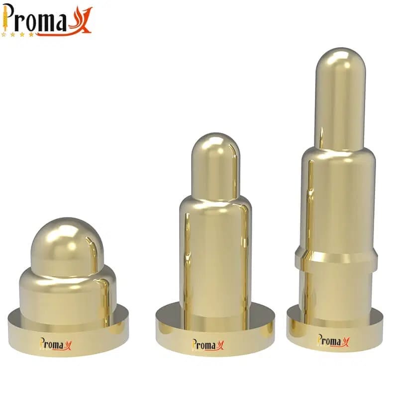
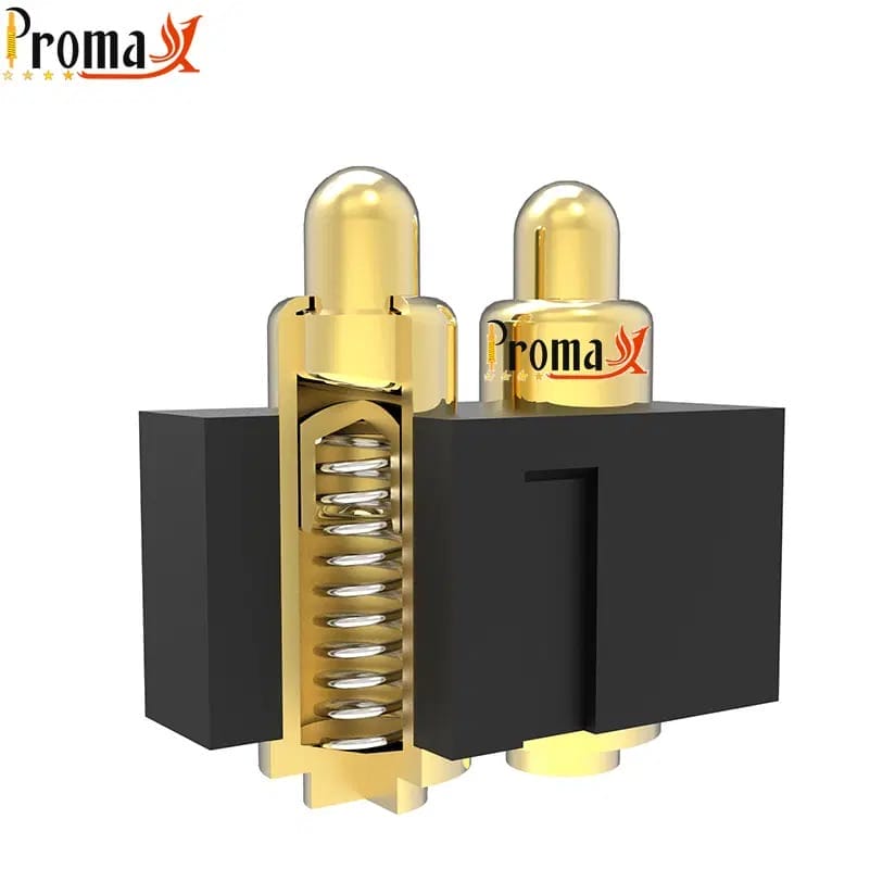
A pogo pin contact holds an electrical connection by pressing against a surface rather than being soldered to it. Three parts do the work inside spring-loaded pogo pin contacts: a plunger, a barrel, and a compression spring. How those parts are built, and what they’re made of, decides how the connection behaves in a finished product.
The pad on the other side carries just as much weight, and it usually gets specified last. What follows covers the anatomy, the materials, the spring mechanism, and how to design the landing pad that meets the pin.
What Is a Pogo Pin Contact?

A pogo pin contact is a spring-loaded electrical contact built from a plunger, a barrel, and a compression spring. The spring pushes the plunger outward, and that push holds the connection against a mating surface without a soldered joint. Because the plunger moves, the contact absorbs misalignment and height variation that a rigid pin cannot. Designers reach for them wherever two parts need to connect and separate repeatedly.
The table below sets out what each part does, what it’s commonly made of, and what that means on your side of the design.
| Part | What it does | Common material direction | What it changes for your design |
|---|---|---|---|
| Plunger | Moves through the stroke and touches the mating surface. | Brass or Beryllium Copper, plated. | Tip shape decides how the contact sits on a pad and how both sides wear. |
| Barrel | Guides the plunger and carries most of the current. | Brass, with stainless steel where side load is a concern. | Wall thickness shows up in the current rating and in how the pin survives off-axis force. |
| Spring | Pushes the plunger out and holds force across the stroke. | Spring steel, stainless steel, or Beryllium Copper on higher grades. | Spring rate sets contact force, which sets how steady the connection stays under vibration. |
| Bias feature | Pushes the plunger sideways against the barrel wall to keep the current path in metal-to-metal contact. | An angled tail, a ball, or an internal clip. | Keeps current running through the barrel rather than the spring coil, which stabilizes resistance over the life of the part. |
| Mating target or pad | The fixed half the plunger lands on. | A plated board pad, a target pin, or a discrete contact disc. | Its size, finish, and flatness matter as much as anything inside the pin. |
How the three parts share the work
Each part has one main job, and they only work as a set. The spring supplies force, so it decides how hard the plunger presses. The barrel guides that movement and carries most of the current through the pin. The plunger does the touching, which makes its tip the part that wears first.
Swap any one of them, and the other two absorb it. A stiffer spring raises contact force, which helps under vibration and wears the plating faster on both halves.
Contact, connector, or probe
These words get mixed up in datasheets and purchase orders, so they’re worth separating. A pogo pin contact is the single part: one plunger, one barrel, and one spring. Pogo pin contacts assembled into a housing at a set pitch become a connector. The same part built for repeated test work, with a harder tip and tighter control on force, is a test probe.
What Are the Components Made Of?
No alloy wins across the board. Every choice trades conductivity against strength, cost, or fatigue life, and the right call depends on what the contact has to survive. Pick for the job the part actually does, not for the best line on a spec sheet.
Plunger alloys and tip geometry
Brass covers most consumer work. It machines cleanly, conducts well, and keeps tooling costs down at volume. Beryllium Copper costs more, and it earns that on parts that flex or cycle hard—it holds its shape far longer under repeated load.
Tip shape matters as much as the alloy. A flat tip spreads load across a pad and keeps wear even, which suits charging contacts on a smooth landing. Crown tips bite through light contamination, so they hold up better on surfaces that see handling. Pointed tips concentrate force into a small area, which helps in test work and is harder on the pad underneath.
Barrel alloys and wall thickness
Brass shows up again here for the same reasons, and stainless steel takes over where side load is a real risk. Wall thickness is the quiet variable behind a current rating. Thicker walls carry more current and resist bending, and they push the outside diameter up, which costs board space.
That trade lands early in a layout. A pin sized for current can force a wider pitch. A pitch set for density can cap how much current the part will take. Copper alloy demand across the connector industry tracks this dynamic—a shift documented by Grand View Research.
The spring: material and why it does not conduct
Springs get chosen for force and fatigue life, not for conductivity. Spring steel and stainless steel cover most designs. Beryllium Copper appears where the spring itself needs to resist corrosion.
Current sent through a coiled spring takes a long, thin path with poor contact between the coils. That is why the barrel carries the load instead and why the bias feature described in the next section exists at all.
Plating stacks
Gold plating over a Nickel underplate is the working default for contact surfaces. Gold resists tarnish and keeps the interface stable. The Nickel layer blocks base metal from migrating up into the Gold, and slows the softer layer from wearing through.
ASTM B488 sets out gold coating types by purity and hardness and covers when a Nickel underplate belongs on a given substrate. Ask a supplier which type they are quoting, not just a thickness. What they can hold depends on the part size, the alloy underneath, and their own plating line.
How Does the Spring Mechanism Work?
The action is straightforward. The plunger compresses, the spring pushes back, and the connection holds because that push never stops. What makes it reliable or not is everything arranged around that push.
Stroke and working travel
Total travel is the full mechanical range the plunger can move. Working travel is the narrower band inside it where spring force stays predictable and the contact stays stable.
Board spacing gets set against working travel, not against the maximum. Push a pin to the bottom of its stroke, and force climbs sharply, which fatigues the spring and can flatten it over time. Leave it barely compressed, and force may drop below what the connection needs under vibration.
What the bias feature actually does
A spring is a poor conductor, so the current needs a path that avoids it. That is the job of the bias feature. An angled plunger tail, a ball, or an internal clip all do the same thing: each pushes the plunger sideways against the barrel wall, holding metal against metal through the stroke.
Without that sideways push, the plunger can float in the bore, and the electrical path wanders with it. Contact behavior then changes with orientation and vibration—a fault that is difficult to trace in the field. At Promax Pogo Pin, our engineers select the bias arrangement against the current and the mounting orientation. A design that behaves correctly upright can behave differently on its side.
Wipe action
As the plunger seats, it moves slightly across the pad. That small scrub is a wipe action, and it clears light films and oxide off the landing surface each time the connection is made. A contact that remains under constant pressure without mating and unmating often performs worse than one that wipes on every connection. Vibration without wiping grinds the same spot, which is the mechanism behind fretting. IEC 60512-2-5 tests for exactly that behavior under movement.
All of these choices show up as contact resistance, measured under the millivolt method described in IEC 60512-2-1. How resistance drifts across a part’s life is covered in our guide to how contact resistance behaves over time.
Need pogo pins fast? Talk to an engineer
Get a custom quote, spec matching, and manufacturing guidance—without slowing down your project.
- ISO 9001 / 14001 / 45001 + IECQ QC080000
- 15+ years of expertise
- Free samples
- Mass production in 15–20 days
How Do You Design the Mating Contact Pad?

Half the connection sits on the board, and it’s the half that usually gets specified last. A pad is easy to treat as a copper shape with a finish on it, and that is how a well-chosen pin ends up performing badly. The plunger can only be as good as what it lands on.
The four decisions below each require prose reasoning. Three further checkpoints—mask definition, vias in the landing zone, and surface condition—are covered in Table 2.
Sizing the pad against the tip
Leave a margin around the tip so the contact lands inside the plated area every time. That margin absorbs housing tolerance, assembly misalignment, and whatever the alignment scheme does not catch.
When the tip finds the pad edge, the contact area shrinks, the plunger can tilt slightly, and the connection changes from one mate to the next. Troubleshooting usually starts at the pin, which is the wrong end of the problem.
Surface finish on the pad side
A flat, hard, corrosion-resistant finish suits a wiping contact. Electroless Nickel Immersion Gold (ENIG) gives that surface and stays flat across a board.
Hot Air Solder Leveling (HASL) leaves height variation instead. Across an array of pins, that variation turns into uneven compression, as some pins sit deep in their stroke while others barely touch. On a single contact, you may never notice it. On six in a row, it shows up as intermittent behavior on whichever pin got the low spot.
Pairing the pad plating with the pin plating
Keep the pad plating in the same family as the pin plating. Two dissimilar metals pressed together, with any moisture present, set up a galvanic cell at the interface and corrode.
This point rarely appears in competitor guides, and it is a common way a good pin and a good board fail together. Gold-plated pins want a Gold-plated landing. Where the board finish is already fixed for other reasons, say so early—the pin plating can then be matched to it rather than the reverse.
Flatness and coplanarity across an array
With one pin, parallelism barely matters. With several, it decides whether they all reach working travel together.
Housing stiffness, board thickness, and pin count all feed into it. A thin board can bow under the load of a multi-pin array, lifting the center pads away from the pins. Solving that in the mechanical design costs far less than compensating with spring force. For the layout side, our footprint and assembly guidance cover the manufacturing detail.
The table below collects the pad decisions in one place, with what each one depends on and how it signals a problem when it drifts.
| What you set | Practical direction | What it depends on | What shows up when it drifts |
|---|---|---|---|
| Pad size against the tip | Leave a margin around the tip so the contact lands inside the plated area every time. Around 0.5 mm of extra diameter is a common starting point. | Housing tolerance, array size, and alignment scheme. | The tip catches the pad edge, and the connection changes between mates. |
| Surface finish | A flat, hard, corrosion-resistant finish suits a wiping contact. | Cycle count, current, and board finish are already specified. | Finishes with height variation leave some pins compressed and others barely touching. |
| Plating pairing | Keep the pad plating in the same family as the pin plating. | Both suppliers’ plating specs. | Dissimilar metals at the interface invite galvanic corrosion. |
| Flatness and coplanarity | Keep the two mating faces parallel across the whole array. | Pin count, housing stiffness, and board thickness. | Uneven compression, with the outer pins carrying the load. |
| Mask definition | Keep the solder mask off the landing area. | Fab capability and pitch. | The plunger rides the mask edge instead of the metal. |
| Vias in the landing zone | Keep open vias outside the contact area. | Layer stack and routing density. | The hole traps debris and can tilt the plunger. |
| Surface condition | Specify a smooth, clean landing surface and state how it will be cleaned. | Assembly process and operating environment. | Contact behavior that wanders from cycle to cycle for no visible reason. |
Please note that these are starting points. What a board house and a pin supplier can actually hold depends on the part size, the materials, and their own process control.
Which Materials and Platings Fit Your Application?
Material logic gets easier once it’s attached to a real application. The profiles below cover most of what crosses an engineering desk, and each one answers to a different pressure.
Consumer wearables and charging docks
Space and cosmetics run this profile. Small brass barrels with Beryllium Copper plungers suit short travel and tight pad sizes. A lighter Gold layer over Nickel handles a controlled indoor environment. Duty is moderate, so the material budget goes into fit rather than survival.
Medical and instrumentation
Repeatability matters more than raw conductivity here. Beryllium Copper holds fatigue life across long service, and a harder Gold over Nickel survives repeated cleaning without opening up the surface.
Specify against ASTM B488 types so the material trail is documented. Auditors ask for it, and so do customers renewing a contract three years later.
Industrial docking
Vibration, debris, and operators who dock without looking all shape this profile. Heavier barrel walls take the abuse, and stainless steel earns its place wherever side load is real rather than theoretical.
Harder Gold over a fuller Nickel underplate suits environments where contamination is ongoing rather than occasional. Wipe action helps with dirt, so tip geometry that clears film is worth the conversation.
High current and automotive
Heat drives everything in this profile. What matters is the resistance of the whole current path, not the tip alone. Larger diameters and bias designs that widen the internal contact area do the real work. Heavier Gold across the contact zone keeps that path stable as the part ages.
At Promax Pogo Pin, we build custom contacts to 40 A and 120 V where an application calls for it. Each design is matched to the pitch and thermal budget of the project rather than pulled from a catalog. Cycle life depends on spring material, plating, size, and process control together; how those factors interact is covered in our guide to what cycle life actually depends on.
Test and probing
Pad damage is the constraint that shapes this profile. Fine barrels with hardened tips reach tight pitches. Gold over Nickel, with harder Gold on the tip, holds up against the cycle count a fixture demands.
Force gets matched to what the board under test will tolerate—a probe that marks a production board has traded one problem for another.
| Application profile | Plunger and barrel | Plating direction | What drives the call |
|---|---|---|---|
| Wearables and charging docks | Small brass barrels, Beryllium Copper plungers where travel is short. | Gold over Nickel, lighter Gold. | Board space and pad size, with moderate duty and a controlled environment. |
| Medical and instrumentation | Beryllium Copper for fatigue life across long service. | Harder Gold over Nickel, specified against ASTM B488 types. | Repeatable readings after repeated cleaning and a documented material trail. |
| Industrial docking | Heavier barrel walls, stainless steel where side load is real. | Harder Gold with a fuller Nickel underplate. | Vibration, debris, and operators who dock without looking. |
| High current and automotive | Larger diameters and bias designs that widen the internal contact area. | Heavier Gold across the contact zone. | Heat and the resistance of the whole current path, not the tip alone. |
| Test and probing | Fine barrels with hardened tips. | Gold over Nickel, harder Gold on the tip. | How much pad damage the board under test can take against cycle count. |
A pogo pin contact works because the spring, the barrel, the plating, and the pad all hold together across the same stroke. Specify one of them in isolation, and another has to absorb it – that is where most connection faults start.
At Promax Pogo Pin, we build custom pogo pin contacts across brass, Beryllium Copper, and stainless steel barrels, with full control over tip geometry, plating stack, spring force, and bias design.
Send us your board layout and the mating gap. You’ll have engineering feedback within 1–3 days, plus free samples to qualify the part before production.
FAQs on Pogo Pin Contact
Can a pogo pin contact land on bare copper?
A pogo pin contact can touch bare copper, but it should not be designed to. Copper oxidizes, and that oxide layer raises resistance unpredictably within weeks of assembly. A plated landing is the working assumption for any connection meant to last.
Can one connector carry power and data through the same contacts?
Most multi-pin pogo pin connectors carry both, split across separate contacts in the same housing. Pin assignment and spacing decide whether that works: a power line beside a signal line can inject noise. Our engineering team reviews the pin map alongside the layout before a pitch gets locked.
How do you clean a pogo pin contact without damaging it?
Use a soft, lint-free wipe and a solvent matched to the plating. Avoid abrasives and avoid anything that pushes debris down into the barrel, because contamination inside the bore affects travel more than surface dirt affects contact. Aggressive solvents can also attack a lighter Gold coating, so the method depends on how the part was plated.
Do these contacts hold up in sealed or high-temperature housings?
Sealed and high-temperature use is workable, and the answer depends on the spring material and the sealing method. Springs lose force as temperature climbs, which changes contact force in service. Ask a supplier for the rated operating range and the force behavior at temperature, not just a room-temperature figure.
What does a manufacturer need to quote a custom contact?
A quote needs the mating gap, a target contact force, current, expected cycles, the space available, and how the pad is defined. Our engineering team can work from a sketch and a board outline. The more of that list you have up front, the fewer rounds it takes to land on a part.
Back to Top: Pogo Pin Contact: Structure, Materials & Spring Mechanism
Need pogo pins fast? Talk to an engineer
Get a custom quote, spec matching, and manufacturing guidance—without slowing down your project.
- ISO 9001 / 14001 / 45001 + IECQ QC080000
- 15+ years of expertise
- Free samples
- Mass production in 15–20 days