Last Updated on August 10, 2023 by Tony
Ready to blast off into the fascinating world of PCB connectors in High-Density Interconnect (HDI) technology? If you’re a tech-head, an electronics guru, or just curious about the intricacies of PCB design, you’ve landed in the right place. Strap yourself in for a deep dive into HDI technology, where things are complex while the competition is tough.
This electrifying article will unveil the secrets of HDI tech and how PCB connectors are the key to modern electronic devices. From connecting components to space-saving designs, we’ll discover how HDI tech and PCB connectors deliver high-performance, compact, and affordable solutions that are game-changers.
We’ll also arm you with tips and insights to unlock HDI tech’s full potential and create unique designs. Whether you’re an old pro or a rookie, prepare to rev up your skills with our must-read guide to PCB connectors in HDI tech. Buckle up, and let’s blast off!
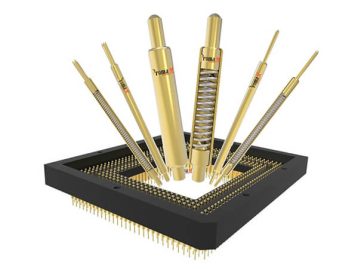
Common PCB Connectors in HDI Technology
Here’s a rundown of the three most common types of PCB connectors:
| Connector Type | Features | Suitable Applications |
|---|---|---|
| Edge Connectors | High-speed data transfer, low signal loss, fragile | Servers, routers, graphics cards, etc. |
| Surface-Mount Connectors | Small size, low cost, easy automated assembly | Smartphones, tablets, gaming consoles, etc. |
| Through-Hole Connectors | High strength, resistant to harsh environments, easy repair | Industrial equipment, medical devices, etc. |
Edge connectors are like the connectors you see in computer memory modules. They have metal contacts or pins that fit into matching slots or sockets on an external device. They are great for high-speed data transfer, such as in servers, routers, and graphics cards.
Their low signal loss and high signal integrity make them suitable for applications where data transfer speed is crucial. However, they can be fragile and prone to damage from repeated insertion and removal, making them unsuitable for some applications.
SMT connectors are mounted directly onto the surface of a PCB using solder paste and a reflow oven. With a compact size and a low profile, they are ideal for consumer electronics like smartphones, tablets, and gaming consoles.
SMT connectors are easy to assemble and can be automated using pick-and-place machines, which makes them a popular choice. However, they can be more susceptible to failure due to thermal stresses on the solder joints. It makes them less reliable than other connector types for some applications.
Through-hole connectors are the connectors you see in industrial equipment or medical devices. They’re mounted onto a PCB by inserting metal pins through holes in the board and soldering them on the opposite side. They are robust and resistant to mechanical stress, which makes them ideal for harsh environments and high-vibration applications.
They’re also relatively low-cost and can be easily repaired or replaced. But, they require holes in the PCB, which can increase the manufacturing cost and complexity. They’re also larger than SMT connectors, making them unsuitable for space-constrained applications.
Choosing PCB Connectors for HDI Technology
To choose the best-suited PCB connectors for high-density interconnect (HDI) technology, there are several factors to consider including the following:
| Considerations | Advantages of Connector A | Advantages of Connector B |
|---|---|---|
| Electrical and Mechanical Requirements | High current and voltage rating | Small size and high-speed signal transmission |
| Environmental and Operating Conditions | Corrosion resistance, waterproofing, high-temperature tolerance | Vibration resistance, suitability for harsh environments |
| Cost and Availability | Low cost, easy availability | Higher reliability, the lower failure rate |
| Industry Standards and Regulations | Compliance with industry standards and regulations | Compliance with industry standards and regulations |
-
Electrical and Mechanical Requirements
When selecting PCB connectors for HDI technology, consider their electrical and mechanical requirements. It includes the number of pins, pitch, current rating, and voltage rating, and the connector’s physical dimensions, shape, and mounting method. It must be considered to ensure the connector meets your application requirements.
-
Environmental and Operating Conditions
Consider the environmental and operating conditions the connector will be exposed to. It includes factors such as temperature, humidity, shock, and vibration. Depending on the application, you may need connectors offering corrosion, water, dust, or chemical resistance. Choose connectors that can withstand your application’s environmental and operating conditions to ensure reliable performance.
-
Cost and Availability
Availability and cost are significant considerations when choosing PCB connectors. Some connectors may be unavailable somewhere or more expensive than others. Balance the cost and availability of the connector with your application’s requirements to get the best value for your money.
-
Industry Standards and Regulations
Also, consider industry standards and regulations when selecting PCB connectors for HDI technology. Different industries may have diverse standards and regulations to dictate the type of connectors. These standards and regulations can relate to safety, EMI (electromagnetic interference), and compatibility, among other factors. Choosing connectors that comply with these standards and regulations is essential to ensure your application meets the specific requirements.
Best Practices for Using PCB Connectors in HDI Technology
To guarantee the best performance and reliability when using PCB connectors in high-density interconnect (HDI) technology, follow these best practices:
1. Design Considerations
When designing a PCB layout and routing for connectors in HDI technology, there are two key factors to consider:
-
PCB Layout and Routing
The PCB layout and routing should be optimized to cut signal loss and ensure proper signal integrity. It includes minimizing the distance between the connector and the components it’s connecting, reducing the number of vias and signal paths, and using the proper trace width and spacing.
-
Signal Integrity and EMI/RFI
Consider signal integrity and electromagnetic interference/radio frequency interference (EMI/RFI) when designing a PCB layout and routing. It includes using proper grounding techniques, minimizing crosstalk between traces, and shielding and filtering components where necessary.
2. Assembly and Manufacturing
When it comes to assembly and manufacturing, there are two key factors to consider:
-
Quality Control and Inspection
Have quality control measures in place during manufacturing to ensure the connectors are assembled and installed. It includes inspecting the connectors for any damage or defects, verifying the pin connections, and ensuring the connectors are properly secured to the PCB.
-
Testing and Verification
Once the PCB connectors are assembled and installed, test and verify their performance. It includes performing electrical tests, such as continuity and resistance checks, and functional tests, such as signal integrity and EMI/RFI testing. You can ensure reliable performance at the best prices by following these best practices for using PCB connectors in HDI technology.
Examples of PCB Connectors in HDI
To understand the practical applications of PCB connectors in HDI technology, let’s take a look at some real-world examples:
| Application Field | Features | Connector Type |
|---|---|---|
| Smartphone and Mobile Devices | Small size, high-speed data transfer, enhanced user experience | Surface-Mount Connectors |
| Medical Devices and Healthcare Applications | Reliability, performance, and safety requirements | Through-Hole Connectors |
| Autonomous Vehicles and Transportation Systems | Complex sensor networks, high-speed data transfer, durability | Edge Connectors |
-
Smartphone and Mobile Devices
PCB connectors play a critical role in the compact and complex designs of smartphones and other mobile devices. These devices need small, reliable, and high-speed data transfer connectors. HDI technology enables micro via and fine-pitch designs to increase density and improve performance in these connectors. Thus, PCB connectors in mobile devices have enhanced functionality, data transfer rates, and user experience.
-
Medical Devices and Healthcare Applications
PCB connectors are used in numerous medical devices and healthcare applications, including imaging systems, monitoring devices, and diagnostic equipment. These connectors must meet strict reliability, performance, and safety requirements.
HDI technology allows diminutive and reliable connectors, crucial for medical devices with limited space. Successful implementation of PCB connectors in healthcare applications has led to more accurate and efficient diagnosis and treatment.
-
Autonomous Vehicles and Transportation Systems
They are essential in autonomous vehicles and transportation systems. This is because these systems rely on complex sensor networks and high-speed data transfer. Harsh environmental conditions, including moisture, vibration, and extreme temperatures, necessitate that the connectors are durable and robust.
HDI technology allows the design of connectors that can meet these requirements while also being compact and lightweight. As such, PCB connectors in transportation systems have improved safety, efficiency, and reliability. These examples show the versatility and importance of PCB connectors in HDI technology.
Common Challenges and Issues with PCB Connectors in HDI Technology
Despite the advantages and benefits of PCB connectors in HDI technology, some common challenges and issues can arise. So, be aware of these challenges and take the necessary steps to address them to ensure the reliable operation of your PCB connectors.
| Challenges and Issues | Solutions |
|---|---|
| Signal Integrity and Crosstalk | Optimizing PCB layout and routing design, using connectors with appropriate shielding and impedance |
| Thermal Management | Using connectors with high current-carrying capacity and effective heat-sinking and cooling methods |
| EMI/RFI Interference | Using connectors with proper grounding and shielding, and implementing effective filtering techniques |
-
Signal Integrity and Crosstalk
High-speed data transfer in HDI technology requires connectors to maintain signal integrity and reduce crosstalk. But, as connector density increases, signal integrity can be compromised due to impedance mismatches and reflections. Crosstalk can also occur due to electromagnetic coupling between adjacent conductors. Effectively dealing with these challenges necessitates meticulous PCB layout and routing design and using connectors with suitable shielding and impedance.
-
Thermal Management
HDI technology often involves high-density connectors that generate heat. It particularly can cause issues with thermal management. As such, thermal stress by this heat can lead to gradual degradation and eventual failure of electronic systems. Overcoming these challenges requires connectors that offer high current-carrying capacity and low contact resistance with effective heat-sinking and cooling methods.
-
EMI/RFI Interference
EMI/RFI can cause issues with the performance and reliability of PCB connectors in HDI technology. A range of factors can lead to EMI/RFI interference, impacting the signals’ quality and reliability.
They include nearby electronic devices or equipment and poor grounding or shielding of the connectors. To tackle these challenges, using connectors with appropriate grounding and shielding and effective filtering techniques is crucial.
-
Other Challenges
Other common challenges with PCB connectors in HDI technology include reliability issues due to non-compliant or counterfeit connectors, compatibility issues with different connector types and standards, and challenges with installation and maintenance.
By being aware of these challenges and taking the necessary steps to address them, you can ensure the reliable operation of your PCB connectors in HDI technology.
Future Trends and Innovations in PCB Connectors for HDI Technology
As technology continues to advance, PCB connectors are also evolving, ushering in new trends and innovative solutions. Here are some of the future trends and innovations to watch out for:
-
Emerging Technologies and Applications
With the progress of technology, new uses for PCB connectors in HDI technology are being created. These applications include IoT, wearable devices, and autonomous vehicles. They need compact and reliable connectors to handle fast data transfer and harsh conditions.
-
Materials and Manufacturing Processes
New materials and ways of manufacturing are driving progress in PCB connectors for HDI technology. Materials like flexible substrates and conductive inks allow flexible and bendable connectors, while 3D printing makes it simpler to create intricate designs.
-
Standardization and Compatibility
Standardization and compatibility are vital trends in PCB connectors for HDI technology. With the rising number of connectors, it’s crucial to develop standardized connector designs and interfaces that can be seamlessly integrated into various systems and equipment. It will ultimately decrease costs and improve interoperability.
-
Advanced Testing and Verification
Moreover, advanced testing and verification methods are being created to guarantee the reliability and performance of PCB connectors in HDI technology. Let’s take X-ray inspection and thermal imaging. They are now used to detect defects and failures in connectors that may not be easily seen by the naked eye.
Conclusion
PCB connectors play a crucial role in High-Density Interconnect (HDI) technology. They provide reliable and efficient electrical connections in tight spaces. Thus they enable the development of smaller and more sophisticated electronic devices.
The key to success in HDI technology lies in selecting the suited connectors that meet the specific requirements of your design. They can be the missing piece that unlocks the full potential of your design and allows it to reach new heights of innovation. So, take the time to research and check your options carefully, but don’t settle for the second best.In a world where technology is advancing at breakneck speed, staying ahead of the curve is more important than ever.
With HDI technology and the appropriate PCB connectors, you can achieve your goals faster, cheaper, and more efficiently than ever. So, innovate, and may your designs be as brilliant as the connectors that power them.