Over 15 Years of Expertise
 FREE samples provided to ensure product satisfaction
 Rapid Turnaround: Mass Production Complete in 15 - 20 Days
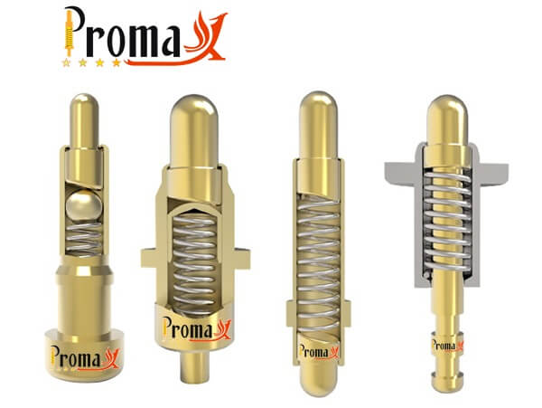
Efficiency, cost-effectiveness, and flexibility are paramount in the dynamic world of electronic prototyping. PCB pogo pins, a groundbreaking innovation, are set to transform electronic prototyping. Let’s explore what they are, why they matter, and the significant changes they bring.
Traditional prototyping involves time-consuming soldering, design limitations, and rising material expenses.
The need for a faster, cost-efficient, and flexible solution prompts a shift in prototyping methods. Enter PCB pogo pins – the game-changer in electronic prototyping.
This article will delve into what sets them as the solution to the limitations of conventional methods. So why wait? Let’s have this deal!
What Are PCB Pogo Pins?
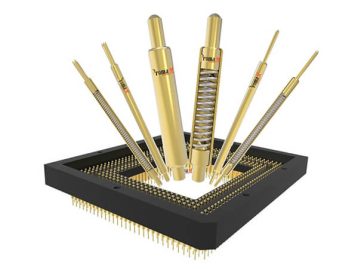
PCB Pogo Pins, or spring-loaded contacts, are specialized connectors for temporary electrical connections in electronic prototyping.
These pins, featuring a spring-loaded mechanism, allow for reliable electrical connections without soldering, simplifying the prototyping process.
Significance
The significance of PCB Pogo Pins lies in their ability to revolutionize electronic prototyping. Unlike traditional soldering methods, these pins provide a faster and more flexible alternative, ensuring a reliable and consistent connection.
They address challenges associated with soldered joints, enhancing overall reliability and reducing prototyping costs by eliminating the need for soldering materials.
Working Principle
PCB Pogo Pins operate on a spring-loaded design with a plunger, spring, and housing. When pressure is applied, the plunger compresses against the spring, creating a temporary electrical connection. Upon release, the spring extends, breaking the connection.
This dynamic mechanism allows quick and reliable connections without the permanence of soldering, making PCB Pogo Pins essential for streamlined prototyping.

Understanding the Electronic Prototyping Process
Electronic prototyping creates initial versions of electronic devices for design testing before mass production. This process refines ideas, identifies issues, and ensures the final product functions. Here are the key steps:
- Conceptualization: Start with a clear idea of the device, defining its purpose, features, and functionality. Brainstorm, sketch, and outline initial specifications.
- Schematic Design: Create a detailed diagram showing electronic component connections. This serves as a roadmap for the physical circuit layout on the PCB.
- Component Selection: Carefully choose components based on performance, size, power, and cost. Ensure compatibility and availability.
- PCB Layout: Translate the schematic into a physical layout on the PCB using specialized software. Consider factors like signal integrity and thermal management.
- Prototyping Board Assembly: Assemble components on a prototyping board for quick modifications and testing before committing to a permanent design.
- Testing and Iteration: Systematically test the prototype, addressing issues and making adjustments for optimal performance.
- PCB Fabrication: Move to fabricating the actual PCB using specialized manufacturing processes.
- Component Mounting: Mount electronic components onto the fabricated PCB precisely for proper alignment and soldering.
- System Integration: Integrate additional components or subsystems into the PCB, verifying communication and functionality.
- Final Testing: Thoroughly test the assembled device to validate performance, reliability, and adherence to design specifications.
- Documentation: Document the entire process, including schematics, layouts, component lists, and testing results for troubleshooting and future reference.
Understanding these steps is crucial for bringing electronic devices from concept to reality.
Benefits of PCB Pogo Pins in Electronic Prototyping
Streamlined Prototyping
PCB Pogo Pins revolutionize prototyping, speeding up circuit assembly and disassembly.
Unlike time-consuming soldering, these pins allow quick component interchange, facilitating rapid design iterations and reducing prototyping time.
Enhanced Reliability
Reliability is key in electronic connections, and PCB Pogo Pins excel in providing consistent and trustworthy links.
The spring-loaded mechanism ensures a secure connection, minimizing troubleshooting and ensuring circuit integrity—critical in precision-demanding applications.
Improved Design Flexibility
PCB Pogo Pins enhance design flexibility by eliminating constraints seen in traditional methods.
Designers can easily reconfigure circuits without intricate soldering, encouraging exploration and optimization of design possibilities. This flexibility is crucial for scenarios requiring rapid adjustments.
Reduced Prototyping Costs
Cost-effectiveness is a hallmark of PCB Pogo Pins. By eliminating consumables like solder and wires, they significantly reduce prototyping expenses.
Their reusable nature contributes to cost savings, and the streamlined process reduces labor costs associated with complex soldering tasks.
Advantages Over Traditional Methods
PCB Pogo Pins offer distinct advantages compared to traditional methods, like soldering and wire wrapping. Eliminating soldering reduces the risk of cold solder joints, ensuring a robust connection.
The reversible nature allows quick adjustments, promoting an agile and responsive prototyping workflow—a paradigm shift in electronic prototyping.

Applications of PCB Pogo Pins in Electronic Prototyping
PCB Pogo Pins, vital in electronic prototyping, excel in diverse scenarios, enhancing testing, verification, evaluation, and education.
PCB Testing and Debugging
Pivotal in testing and debugging, Pogo Pins’ spring-loaded design ensures swift, reliable connections between boards and test equipment. In manufacturing or development, they streamline testing, aiding prompt issue identification and resolution.
Circuit Design Verification
In electronic prototyping, Pogo Pins offer a rapid solution for verifying circuit designs. They enable real-time validation by facilitating quick connections to different circuit parts, ensuring performance according to specifications and fostering efficient iterations.
Component Evaluation
Pogo Pins simplify component evaluation during prototyping. Their versatility allows engineers to efficiently swap components and test various configurations, ensuring the selected components meet project requirements.
Educational Prototyping
In educational settings for electronics and circuit design, Pogo Pins offer a versatile, accessible, and reusable platform. Ideal for hands-on learning, they introduce students to prototyping intricacies without the complexities of traditional methods.
PCB Pogo Pins transcend mere connectivity, serving as efficient tools in electronic prototyping—from testing and debugging to educational exploration. Their adaptability makes them indispensable in the engineer’s toolkit.
Integrating PCB Pogo Pins into Your Electronic Prototyping Workflow
Efficiently incorporating PCB Pogo Pins into your electronic prototyping workflow involves a strategic process.
1.Selecting the Right PCB Pogo Pins
- Choose Pogo Pins based on key factors like size, pitch, spring force, and current rating. Tailor these specifications to match your prototyping project’s needs, ensuring optimal connectivity for devices of any size.
2.Designing PCB Layouts
- Craft PCB layouts with careful consideration for Pogo Pin integration. Ensure proper alignment, adequate spacing, and seamless electrical connections. A well-thought-out PCB design enhances the efficiency of Pogo Pin integration, promoting smooth and reliable connections.
3.Implementing PCB Pogo Pins
- Translate your design and Pogo Pin selection into a tangible prototype. Provide practical tips for implementing Pogo Pins, covering various connection techniques and troubleshooting methods.
- Pay close attention to the accurate alignment of Pogo Pins with corresponding components, and offer guidance on effective soldering or press-fit techniques to bolster connection robustness.
Effectively integrating PCB Pogo Pins into your prototyping workflow demands a holistic approach, from careful selection to thoughtful implementation.
It ensures you harness the advantages of Pogo Pins, such as rapid prototyping, enhanced reliability, and cost-effectiveness, in your projects.

Future of PCB Pogo Pin Technology in Electronic Prototyping
The electronic prototyping field is ever-changing, and the future of PCB Pogo Pin technology is promising.
As technology evolves and the demand for quicker, more efficient prototyping grows, key trends and innovations shape the path of PCB Pogo Pins.
Emerging Technologies
Stay updated on technologies influencing PCB Pogo Pin applications. 5G, Internet of Things (IoT), and miniaturization advances will likely impact the design and function of Pogo Pins.
As devices get smaller and more connected, Pogo Pins become essential for rapid prototyping in these cutting-edge technologies.
Potential Impact on Prototyping
Anticipate how PCB Pogo Pin technology can impact electronic prototyping. Innovations in design, materials, and manufacturing may lead to faster cycles, improved reliability, and enhanced versatility.
Consider how these advancements align with your specific prototyping needs, streamlining your workflow.
Challenges and Solutions in PCB Pogo Pin Implementation
Using PCB Pogo Pins for electronic prototyping has great advantages, but it comes with its challenges. Recognizing and addressing these challenges is crucial for a smooth and productive prototyping process.
Common Challenges
In PCB Pogo Pin implementation, issues like alignment problems, inconsistent connections, or selecting the appropriate pins for specific applications can occur. Identifying these challenges early allows for proactive solutions.
Maintenance Issues
Like any mechanical component, Pogo Pins need regular maintenance for optimal performance. Common problems include wear, oxidation, or contamination.
A routine maintenance schedule and following cleaning and inspection guidelines can extend Pogo Pins’ lifespan.
Troubleshooting Problems
Prototyping projects may face issues, including intermittent connections or difficulty identifying faulty Pogo Pins.
A systematic troubleshooting approach involving checking connections, inspecting pins, and using diagnostic tools can speed up issue identification and resolution.
Effective Solutions
Solving challenges requires proper planning, strategic pin selection, and following maintenance best practices.
Addressing alignment issues might involve redesigning the PCB layout or using self-aligning Pogo Pins. Inconsistent connections can be reduced by selecting pins with suitable spring forces and materials.
Maintenance Guidelines
Clear maintenance guidelines are crucial for Pogo Pins’ performance. Recommendations for cleaning, lubrication, and periodic inspection ensure reliable operation over time.
Troubleshooting Techniques
Equip your team with troubleshooting techniques for swift issue resolution during prototyping.
Techniques include using multimeters for continuity testing, visually inspecting for damage, and employing specialized tools for in-depth diagnostics.

Conclusion
Integrating PCB Pogo Pins enhances efficiency, reliability, and cost-effectiveness in electronic prototyping. These pins streamline prototyping, enabling quick design iterations and accelerated product development.
When incorporating PCB Pogo Pins, choose wisely, design layouts thoughtfully, and implement them effectively. Future advancements in this technology promise to reshape electronic prototyping.
While challenges may arise, proactive solutions and adherence to guidelines effectively address maintenance and troubleshooting.
For reliable solutions, Promax Pogo Pin Electronics Technology Co., Ltd., a national New High-tech enterprise, specializes in high-quality PCB Pogo Pins, connectors, test probes, and precision sockets, embodying innovation and precision.
Ready to revolutionize your electronic prototyping? Explore the world of PCB Pogo Pins with Promax. Visit Promax Electronics for cutting-edge solutions. Elevate your prototyping process with precision and reliability.