Last Updated on May 23, 2023 by Tony
Do you have a PCB (Printed Circuit Board) that needs to be tested for accuracy and performance? If so, this is going to be the ideal place for you. As we’ve seen, printed circuit boards are the core component of the electronics industry. But how do we know if they’re working properly and free from defects?
That’s where PCB testing comes in. Testing your Printed Circuit Boards (PCBs) is an essential step in the manufacturing process, as it ensures that your product is up to standard and won’t cause any problems down the line. It is a process that ensures the circuit board is functioning correctly and reliably before being used in any application. Testing is done to guarantee the safety, performance, and longevity of the PCB. Without thorough testing, a flawed PCB could lead to product failure and is even dangerous sometimes.
There are a variety of testing methods available to test PCBs, depending on the type of product being tested. Keep reading to learn more about each testing method and how to get the most out of your PCB testing process.
What Is a PCB?
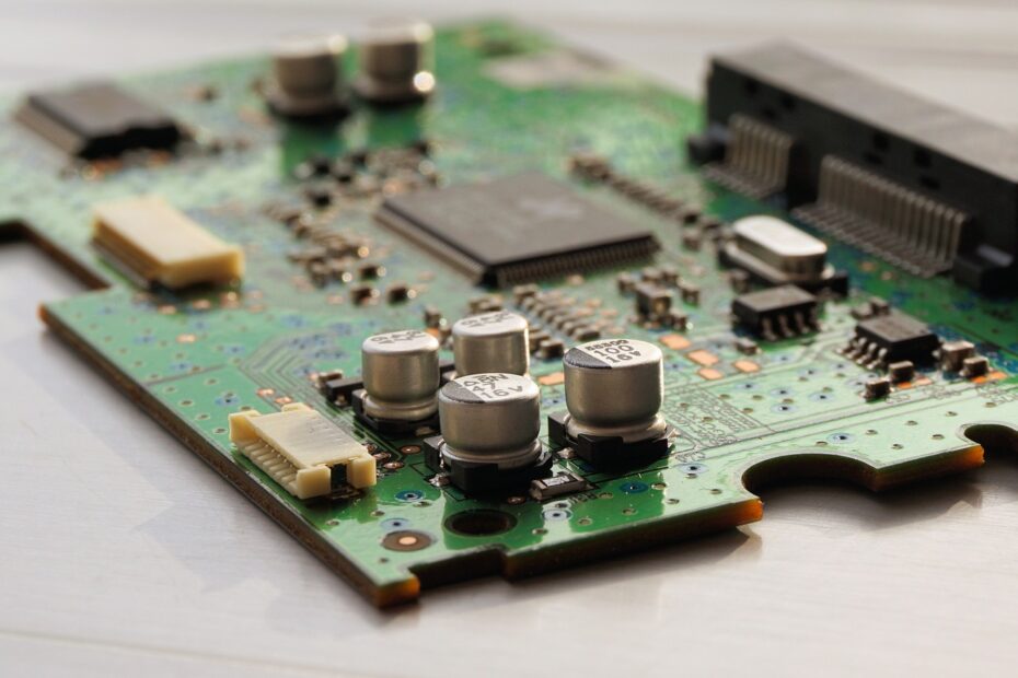
A printed circuit board (PCB) is made of a non-conductive material, such as fiberglass or plastic, and is etched with copper pathways and tracks. These pathways allow electricity to flow from component to component, allowing them to communicate. A wide array of items, such as computers, cell phones, and various appliances rely on PCBs (Printed Circuit Boards).
A PCB is used to hold and connect electronic components. Depending on what product they are being used in, they come in multiple sizes and shapes. The main parts of a PCB are the circuit board, the components, and the solder. These elements should be connected for the PCB to function appropriately. Knowing how these components fit together and how they work is key to understanding how to use a PCB in any project.
Why Do You Need PCB Testing?
There are many benefits to Printed Circuit Board Testing. Some of these benefits include:
-
Eliminating Defects
One of the primary benefits of PCB testing is that it can help eliminate defects in the boards. Also, it can improve the overall quality of the boards and ensure they meet all the requirements.
-
Reducing Costs
It can reduce costs, as it can help ensure the boards are correctly functioning and do not have any defects, leading to less wasted materials and fewer rework costs.
-
Improving Efficiency
PCB testing can also enhance efficiency by improving the quality of the boards, which means that they will not need to be sent back for rework, which can save time and money.
Different PCB Testing Methods
Visual Inspection
Visual inspection PCB testing is a critical step in the PCB manufacturing process. By visually inspecting the PCBs, manufacturers can ensure the boards meet the required specifications and that defects have been identified and addressed. What Visual Inspection Can Do?
- It can detect a wide range of problems, such as missing components, incorrectly positioned components, breaks in the copper traces, and more.
- In addition, visual inspection is also used to check the board for conformance to design rules, as well as to verify that the board is free of contaminants, such as dust and moisture.
By thoroughly inspecting the PCBs, manufacturers can ensure that the boards are of the highest quality and meet all their customers’ expectations.
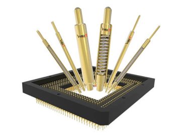
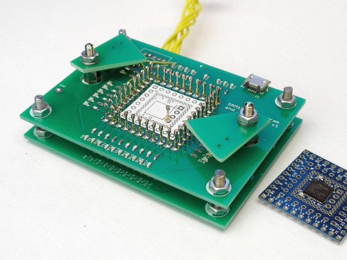
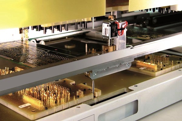
In-circuit Testing
In-circuit testing is one of the most popular methods used for testing printed circuit boards (PCBs). It is based on an electrical connection between the test system and the PCB. During the test, the test system will send electrical signals to the components on the board and compare the results with the expected values. If the results are not within the typical range, the test will fail, and the board will be marked as defective.
This method is used for both debugging and production testing. In-circuit testing can be used to test a wide range of faults, from short circuits and open circuits to component misplacements and other errors in the circuitry. This method is recommended for those who want to ensure the highest quality and reliable PCBs. It can also check the functionality and operability of the PCB. It uses an external power source to test the PCB for functionality. In-circuit testers are used to test both digital and analog circuits.
- Digital in-circuit testing is performed using a bed-of-nails tester. This type of tester has spring-loaded probes that make contact with the test points on the circuit board. The tester checks for proper voltages and continuity between the different points on the circuit board.
- Analog in-circuit testing is performed using an oscilloscope that measures voltage changes over time. The oscilloscope must be connected directly to the points being tested on the circuit board to perform an analog in-circuit test.
Benefits Of In-Circuit Testing MethodThere are several benefits to using in-circuit testing during electronics manufacturing.
- In-circuit testing is quick and easy as it does not require removing the components from the circuit board.
- Moreover, in-circuit testing can identify problems early on in the manufacturing process, which can save time and money by avoiding rework or scrap losses later on down the line.
Functional Testing
Functional testing is a process whereby the functionality of a product is verified. It is done in manufacturing but can also be performed on shipped products. Functional testing of printed circuit boards (PCBs) is critical for quality assurance as it ensures the PCB functions correctly and meets the required specifications. How To Test a PCB Using Functional Testing Method?
- The first step in functional testing is to conduct a visual inspection of the PCB, which includes checking for any visible defects, such as incorrect component placement or broken traces.
- Once the check is complete, the PCB is tested using various methods, such as continuity tests, voltage measurements, and signal integrity tests.
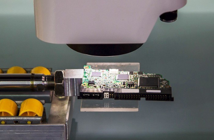
Flying Probe Testing
The flying probe PCB testing method is an advanced testing method used only for high-end PCBs to verify their functionality and quality. It consists of a series of probes to test the electrical connections on the board. The probes can move around the board, which allows them to access and test every area of the board quickly and accurately. The flying probe machine applies pressure on the PCB while checking for faults. Benefits Of Flying Probe Testing
- This method is more efficient than traditional methods because it eliminates the need for manual testing, saving time and money.
- Additionally, flying probe testing is much less tedious and time-consuming, making it the preferred choice for many PCB manufacturers.
- The flying probe testing method is also highly accurate, making it ideal for testing high-density boards and little components.
All in all, this method is invaluable for PCB manufacturers, allowing them to test their boards quickly and accurately.
Automated Optical Inspection (AOI)
Automated Optical Inspection (AOI) uses imaging technology to detect surface defects on printed circuit boards. This is highly efficient and accurate, allowing quality control and defect detection. This type of testing is used to test the appearance of the PCB. AOI is conducted after the PCB has been tested for functionality. The process uses special hardware and software to inspect the PCB for visual flaws, damage, and other issues.
How AOI Testing Method Is Done? AOI utilizes a camera that captures images of the board at high resolutions and compares them to a baseline image. Any discrepancies between the two images are flagged for further review, allowing for quick identification of defects and eliminating the need for manual inspection. Why Use AOI Testing Method?
- AOI also allows for high-speed testing, making it an ideal choice for large-scale manufacturing operations.
- Additionally, AOI can detect defects that are too small to be seen with the naked eye, providing an extra level of assurance and reliability.
- AOI is an excellent choice for manufacturers looking for an efficient and reliable way to test their PCBs.
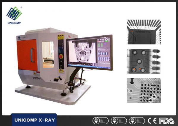
X-ray Inspection
X-ray inspection is a popular and reliable PCB testing method to detect voids, cracks, delaminations, and other defects in printed circuit boards. The process uses a high-resolution X-ray imaging system to capture detailed images of the board, allowing the detection of even the slightest flaws.
This type of testing is used to test the internal structure of a PCB. It is used for high-end PCBs and is done after the PCB has been tested for functionality. This process uses special hardware and software to inspect the PCB for internal flaws and damages. Why Use X-Ray Inspection Method?
- X-ray inspection is a non-destructive test, meaning the board remains intact and can be tested multiple times. Thus, multiple layers of the board can be inspected at once, ensuring the integrity of the board is preserved.
- The combination of speed and accuracy makes X-ray inspection an excellent choice for PCB testing.
- Through quick identification of flaws, this method reduces time and expense in the long term.
- X-ray inspection is also highly sensitive and can detect even the most subtle defects, making it an indispensable tool for quality assurance.
How To Test a PCB Successfully?
- The first step is to determine what type of test you will be performing on the PCB.
- Multiple tests can be performed on a PCB, so it is vital to select the right one for your needs.
- The next step is to collect all the necessary equipment for the test. It may include a multimeter, power supply, and other specialized equipment, depending on the test method type.
- Once everything is set, you may need to connect the PCB to the testing equipment.
- It typically involves connecting leads from the testing equipment to specific points on the PCB.
- After everything is connected, you can begin running the test according to the chosen method.
- Depending on the expected results, this may involve simply monitoring readings or adjusting settings on the testing equipment.
- When the test is complete, you will need to disconnect everything and clean up any mess made during the setup.
- Finally, you should analyze the results and make necessary changes to your design based on your results.
Conclusion
PCB testing is an essential step in the PCB manufacturing and use process. Several different PCB testing methods are available today that offer different levels of accuracy and specificity, so it is vital to choose the suitable testing method for the task at hand when choosing how to test PCBs for quality assurance. We would be glad if you stay connected with us and share your ideas to improve our blog.